3.2 Logic Gates & Circuits
AS Level · 29 questions found
What this topic covers
Section titled “What this topic covers”- Gate symbols and functions: NOT, AND, OR, NAND, NOR, XOR
- Construct truth tables for each gate
- Build a logic circuit from a problem statement, expression or truth table
- Build a truth table from a circuit, expression or problem statement
- Write a logic expression from a circuit, truth table or problem statement
Past paper questions
Section titled “Past paper questions”(a) Draw a logic circuit for the logic expression:
X = NOT ((A NAND B) XOR (NOT A OR NOT C))
(b) Write the logic expression for the following truth table. 2 marks
| R | S | T | Q |
|---|---|---|---|
| 0 | 0 | 0 | 0 |
| 0 | 0 | 1 | 1 |
| 0 | 1 | 0 | 0 |
| 0 | 1 | 1 | 0 |
| 1 | 0 | 0 | 0 |
| 1 | 0 | 1 | 0 |
| 1 | 1 | 0 | 1 |
| 1 | 1 | 1 | 0 |

Q = [2]
Show mark scheme
3(a) [2 marks]
One mark per bullet point, max 2 marks • (A NAND B) and (NOT A OR NOT C) • XOR and NOT
3(b) [2 marks]
1 mark per bullet point, max 2 marks • One correct term: (R AND S AND NOT T) // (NOT R AND NOT S AND T) • Second correct term plus the OR in correct place Answer: Q = (R AND S AND NOT T) OR (NOT R AND NOT S AND T)
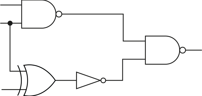
(a) Consider the following logic circuit:
Write the logic expression for the logic circuit. Do not simplify the expression.
X = [2]
(b) Consider the following logic expression: 2 marks
X = NOT ((A NAND B) XOR (NOT A OR NOT C))
A truth table for the logic expression is given:
| Row number | A | B | C | X |
|---|---|---|---|---|
| 1 | 0 | 0 | 0 | 1 |
| 2 | 0 | 0 | 1 | 0 |
| 3 | 0 | 1 | 0 | 1 |
| 4 | 0 | 1 | 1 | 0 |
| 5 | 1 | 0 | 0 | 1 |
| 6 | 1 | 0 | 1 | 0 |
| 7 | 1 | 1 | 0 | 1 |
| 8 | 1 | 1 | 1 | 1 |
There are three errors in the truth table.
Identify the three errors in the truth table by writing the row numbers with an incorrect output.
Error 1 Row number
Error 2 Row number
Error 3 Row number
Show mark scheme
9(a) [2 marks]
1 mark per bullet point, max 2 marks • NOT ( A XOR B ) • NAND (( B AND C ) OR A ) X = (NOT ( A XOR B )) NAND (( B AND C ) OR A ) // X = (( B AND C ) OR A ) NAND (NOT ( A XOR B ))
9(b) [2 marks]
1 mark for 1 or 2 row numbers correct, 2 marks all three correct Row 2 Row 4 Row 7
(a) Complete the truth table for the following logic expression:
X = (A NOR B) NAND (C XOR B)
| A | B | C | Working space | X |
|---|---|---|---|---|
| 0 | 0 | 0 | ||
| 0 | 0 | 1 | ||
| 0 | 1 | 0 | ||
| 0 | 1 | 1 | ||
| 1 | 0 | 0 | ||
| 1 | 0 | 1 | ||
| 1 | 1 | 0 | ||
| 1 | 1 | 1 |
(b) Draw a logic circuit for the logic expression: 2 marks 2 marks
X = NOT (((A AND B) OR C) AND (C NOR D))
X

Show mark scheme
3(a) [2 marks]
1 mark per shaded area, max 2 marks 0 0 0 1 0 0 1 0 0 1 0 1 0 1 1 1 1 0 0 1 1 0 1 1 1 1 0 1 1 1 1 1
3(b) [2 marks]
1 mark per bullet point, max 2 marks • A AND B OR C • C NOR D and final two gates
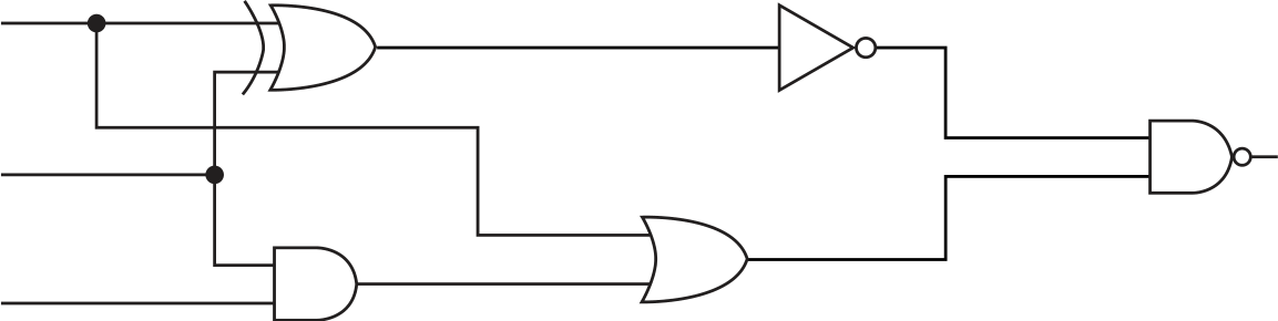
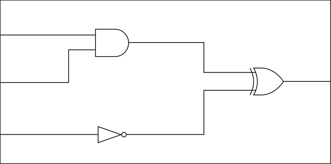
(a) Write the logic expressions for the following logic circuit. 2 marks
Show mark scheme
1(a) [2 marks]
1 mark each: X = Q AND (NOT P OR R) Y = S XOR (Q NOR R)
1(b) [2 marks]
1 mark for first 4 rows, 1 mark for second 4 rows Working space X 0 0 0 1 0 0 1 1 0 1 0 0 0 1 1 1 1 0 0 0 1 0 1 0 1 1 0 1 1 1 1 1
(a) Write the logic expressions for the following logic circuit. 2 marks
| R | X | |
|---|---|---|
| S | S | S |
| S | S | Y |
| T | T | T |
| U | U | U |
| U | U | |
Show mark scheme
4(a) [2 marks]
1 mark each: • X = (R NOR S) XOR T • Y = (T AND U) OR U
4(b) [2 marks]
1 mark for first four rows, 1 mark for second four rows Working space X 0 0 0 1 0 0 1 1 0 1 0 1 0 1 1 1 1 0 0 1 1 0 1 0 1 1 0 0 1 1 1 1
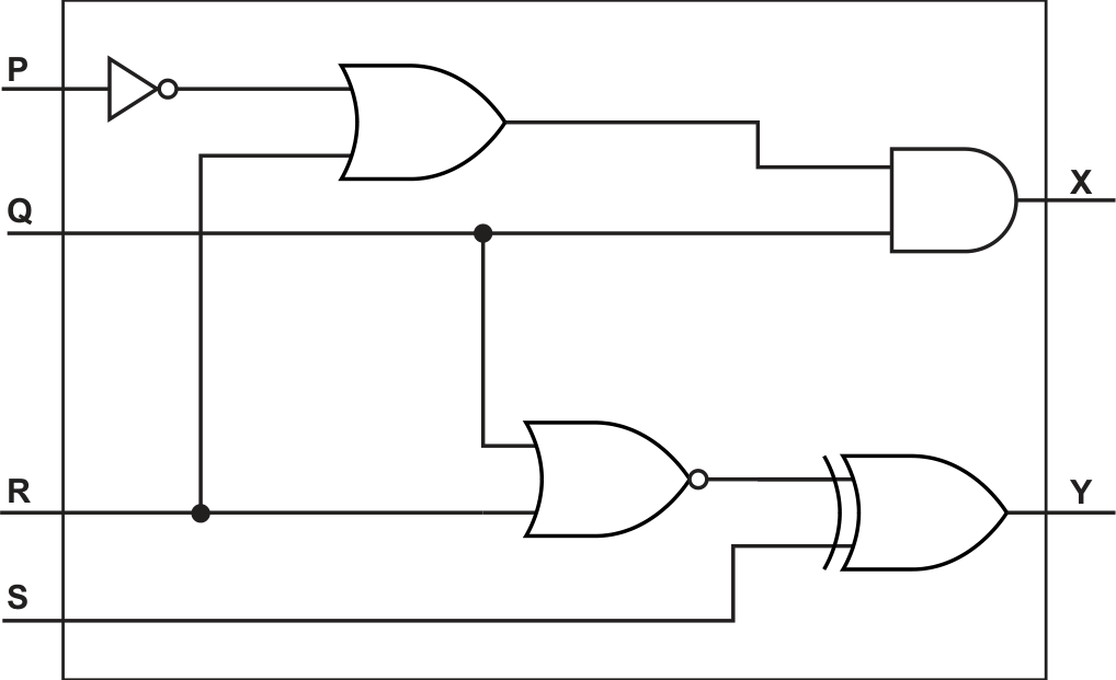
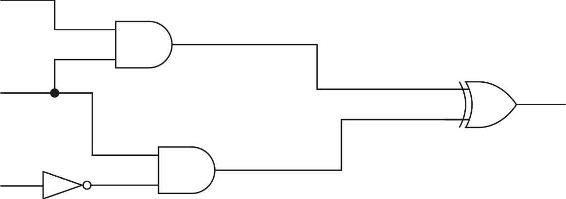
(a) Write the logic expressions for the following logic circuit. 2 marks
(b) Complete the truth table for the logic expression: 2 marks
X = (A OR B) XOR (B OR C) XOR (NOT A NAND C)
| A | B | C | Working space | X |
|---|---|---|---|---|
| 0 | 0 | 0 | ||
| 0 | 0 | 1 | ||
| 0 | 1 | 0 | ||
| 0 | 1 | 1 | ||
| 1 | 0 | 0 | ||
| 1 | 0 | 1 | ||
| 1 | 1 | 0 | ||
| 1 | 1 | 1 |
Show mark scheme
4(a) [2 marks]
1 mark for each correct statement X = B NOR (A NOR C) Y = (B AND C) XOR NOT D
4(b) [2 marks]
1 mark for 1st 4 rows 1 mark for 2nd 4 rows Working space X 0 0 0 1 0 0 1 1 0 1 0 1 0 1 1 0 1 0 0 0 1 0 1 1 1 1 0 1 1 1 1 1
A security system has both a floodlight (very bright light) and an audio alarm.
The data from multiple sensors is analysed and used to:
turn on the floodlight
sound the audio alarm.
Sensors can be used to detect:
if doors are open
the external daylight level
if people are detected within a set distance.
(a) Complete the table to identify the most appropriate type of sensor for each scenario. 1 mark
| Scenario | Type of sensor |
|---|---|
| A door is open. | |
| The external daylight level is below a set amount. | |
| A person is detected within 2 metres. |
(b) The floodlight (X) and audio alarm (Y) operate according to the following criteria: 2 marks
| Parameter | Description of parameter | Binary value | Condition |
|---|---|---|---|
| A | external daylight level | 1 | Low |
| A | external daylight level | 0 | High |
| B | front door | 1 | Open |
| B | front door | 0 | Closed |
| C | person is within 2 m | 1 | Detected |
| C | person is within 2 m | 0 | Not detected |
| D | back door | 1 | Open |
| D | back door | 0 | Closed |
| E | security system | 1 | Switched on |
| E | security system | 0 | Switched off |
The floodlight turns on (X = 1) if:
- the security system is switched on
and
- the external daylight level is low
and
- a person is detected within 2 m.
The audio alarm turns on (Y = 1) if:
- the security system is switched on
and
- one or more doors are open, or a person is detected within 2 m.
Write logic expressions for the security system.
(c) Explain whether the security system is an example of a monitoring system or a control system. 3 marks
Show mark scheme
5(a) [1 mark]
1 mark for all 3 appropriate sensors Scenario Type of sensor A door is open. Pressure sensor // Infra-red The external daylight-level is below a set Light sensor amount. A person is detected within 2 metres. Infra-red
5(b) [2 marks]
1 mark for each correct expression AND A AND AND ( )
5(c) [3 marks]
1 mark for each bullet point ( max 3 ) for a correct justification No marks for the identification of the system Monitoring system • There is no use of feedback // The light and the alarm are just warnings • The output of the floodlight or the audio alarm does not affect the input of data from the sensors • The system does not have any actuators
(a) Complete the truth table for the logic expression: 2 marks
X = (A XOR B) NAND (A AND (B XOR C))
| A | B | C | Working space | X |
|---|---|---|---|---|
| 0 | 0 | 0 | ||
| 0 | 0 | 1 | ||
| 0 | 1 | 0 | ||
| 0 | 1 | 1 | ||
| 1 | 0 | 0 | ||
| 1 | 0 | 1 | ||
| 1 | 1 | 0 | ||
| 1 | 1 | 1 |
(b) Draw the logic circuit for the logic expression: 2 marks
W = P NAND ((Q OR NOT R) XOR (P XOR Q))

Show mark scheme
1(a) [2 marks]
1 mark for each shaded part. 0 0 0 1 0 0 1 1 0 1 0 1 0 1 1 1 1 0 0 1 1 0 1 0 1 1 0 1 1 1 1 1
1(b) [2 marks]
1 mark for (P XOR Q) and (Q OR NOT R) 1 mark for second XOR gate and final NAND gate with appropriate inputs
(a) Describe the operation of a 2-input XOR gate. 1 mark
(b) Write the logic expression for the following logic circuit. 2 marks
(c) Draw the logic circuit for the logic expression: 2 marks
X = ((NOT A AND (B AND C)) OR (B NAND C)) AND NOT A

Show mark scheme
1(a) [1 mark]
1 mark for: Output is only 1 if one input is 1 and the other is 0 // Output is only 1 if both inputs are different // Output is only 0 if both inputs are the same
1(b) [2 marks]
1 mark each: • (( A NOR B ) AND ( )) • NAND ( B AND C ) X = (( A NOR B ) AND ( )) NAND ( B AND C )
1(c) [2 marks]
1 mark for NOT gate, 2 correct AND gates and the NAND gate 1 mark for OR gate and the final AND gate
(a) Tick (✓) one box to identify the correct logic statement for this truth table. 1 mark
| A | B | C | X |
|---|---|---|---|
| 0 | 0 | 0 | 1 |
| 0 | 0 | 1 | 0 |
| 0 | 1 | 0 | 0 |
| 0 | 1 | 1 | 0 |
| 1 | 0 | 0 | 0 |
| 1 | 0 | 1 | 0 |
| 1 | 1 | 0 | 1 |
| 1 | 1 | 1 | 0 |
NOT ( A AND B AND C )
( A XOR B ) NOR C
( A OR B OR C ) NOR C
NOT A AND NOT B AND NOT C
(b) Draw a logic circuit for the logic expression: 2 marks
X = NOT (NOT A AND (NOT B XOR C ))
A
C

Show mark scheme
1(a) [2 marks]
1 mark for: (A XOR B) NOR C
1(b)
1 mark for NOT B XOR C 1 mark for NOT A and final AND plus NOT
(a) Describe the operation of each of the following logic gates: 4 marks
NAND
NOR
XOR
OR
(b) Draw a logic circuit for this logic expression: 2 marks
X = NOT (( A AND B ) OR ( C AND D ))
A
B
X
C
D

Show mark scheme
1(a) [2 marks]
1 mark for each correct answer: NAND The output is 0 when both inputs are 1, otherwise the output is 1 NOR The output is 1 when both inputs are 0, otherwise the output is 0 XOR The output is 1 when one of the inputs is 1 and the other input is 0, otherwise the output is 0 OR The output is 0 when both inputs are 0, otherwise the output is 1
1(b) [4 marks]
1 mark for both AND gates with correct inputs 1 mark for correct OR and NOT gates with correct inputs and no superfluous gates:
Each of the following truth tables has three inputs ( A, B and C ) and one output ( X ).
Draw one line to match each truth table with its logic expression.
Truth table Logic expression
| A | B | C | X |
|---|---|---|---|
| 0 | 0 | 0 | 0 |
| 0 | 0 | 1 | 1 |
| 0 | 1 | 0 | 0 |
| 0 | 1 | 1 | 0 |
| 1 | 0 | 0 | 1 |
| 1 | 0 | 1 | 1 |
| 1 | 1 | 0 | 0 |
| 1 | 1 | 1 | 0 |
| A | B | C | X |
|---|---|---|---|
| 0 | 0 | 0 | 0 |
| 0 | 0 | 1 | 1 |
| 0 | 1 | 0 | 0 |
| 0 | 1 | 1 | 0 |
| 1 | 0 | 0 | 0 |
| 1 | 0 | 1 | 0 |
| 1 | 1 | 0 | 0 |
| 1 | 1 | 1 | 1 |
| A | B | C | X |
|---|---|---|---|
| 0 | 0 | 0 | 1 |
| 0 | 0 | 1 | 1 |
| 0 | 1 | 0 | 1 |
| 0 | 1 | 1 | 1 |
| 1 | 0 | 0 | 1 |
| 1 | 0 | 1 | 1 |
| 1 | 1 | 0 | 0 |
| 1 | 1 | 1 | 1 |
NOT ( A XOR B ) AND C
( A OR C ) AND NOT B
A NAND B NAND C
( A NAND B ) OR C
NOT ( A AND B AND C ) 3 marks
Show mark scheme
6 [3 marks]
1 mark for each correct line:
(a) Complete the truth table for the logic expression: 2 marks
X = NOT ( A NAND B ) XOR (NOT B AND ( B NOR C ))
| A | B | C | Working space | X |
|---|---|---|---|---|
| 0 | 0 | 0 | ||
| 0 | 0 | 1 | ||
| 0 | 1 | 0 | ||
| 0 | 1 | 1 | ||
| 1 | 0 | 0 | ||
| 1 | 0 | 1 | ||
| 1 | 1 | 0 | ||
| 1 | 1 | 1 |
(b) Draw a logic circuit for the logic expression: 2 marks
X = ( A AND NOT ( B OR C )) AND ( B NOR C )
A

B
C
X
Show mark scheme
4(a) [2 marks]
1 mark for each set of 4 rows (shaded) 0 0 0 1 0 0 1 0 0 1 0 0 0 1 1 0 1 0 0 1 1 0 1 0 1 1 0 1 1 1 1 1
4(b) [2 marks]
1 mark for both AND gates 1 mark for NOT gate and OR gate and NOR gate
(a) Write the Boolean expression that corresponds to the following logic circuit.
A B X C 3 marks
(b) Complete the truth table for the logic expression: 2 marks
| X = A | A XOR (B | B AND (A NAND B) AND NOT C) | ||
|---|---|---|---|---|
| A | B | C | Working space | X |
| 0 | 0 | 0 | ||
| 0 | 0 | 1 | ||
| 0 | 1 | 0 | ||
| 0 | 1 | 1 | ||
| 1 | 0 | 0 | ||
| 1 | 0 | 1 | ||
| 1 | 1 | 0 | ||
| 1 | 1 | 1 |
Show mark scheme
4(a) [3 marks]
1 mark for each bullet point • A NAND B • NOT(B XOR C) • Final NAND X = A NAND B NAND (NOT(B XOR C))
4(b) [2 marks]
1 mark for each set of rows (shaded) 0 0 0 0 0 0 1 0 0 1 0 1 0 1 1 0 1 0 0 1 1 0 1 1 1 1 0 1 1 1 1 1
(a) Complete the truth table for the logic expression: 2 marks
| Y | Y = ((P AND Q | Q) XOR ((NOT Q) OR R)) AND NOT P | ||
|---|---|---|---|---|
| P | Q | R | Working space | Y |
| 0 | 0 | 0 | ||
| 0 | 0 | 1 | ||
| 0 | 1 | 0 | ||
| 0 | 1 | 1 | ||
| 1 | 0 | 0 | ||
| 1 | 0 | 1 | ||
| 1 | 1 | 0 | ||
| 1 | 1 | 1 |
(b) Draw a logic circuit for the logic expression: 2 marks
Y = (( P AND Q ) XOR ((NOT Q ) OR R )) AND NOT P
P

R
Show mark scheme
4(a) [2 marks]
1 mark for each set of highlighted rows 0 0 0 1 0 0 1 1 0 1 0 0 0 1 1 1 1 0 0 0 1 0 1 0 1 1 0 0 1 1 1 0
4(b) [2 marks]
1 mark for P AND Q and NOT 1 mark for NOT gate and AND gate and XOR gate
(a) Draw the logic circuit for this logic expression:
T = (NOT A OR B ) XOR ( C NAND D )
A
B
C
D
(b) Describe the function of the NAND and NOR logic gates. 2 marks 2 marks
T

NAND
NOR
Show mark scheme
5(a) [2 marks]
1 mark for 2 gates 2 marks for all 4 gates
5(b)
1 mark each NAND 0 is only output when both inputs are 1 // 1 is only output when none, or (either) one of the inputs is 1 NOR 1 is only output when both inputs are 0 // 0 is only output when (either) one or both inputs are 1
(a) Draw the logic circuit for this logic expression: 2 marks
Z = ( R XOR S ) AND (NOT T NOR P )
R
S
T
P
(b) Complete the truth table for this logic expression: 2 marks
| Z = (NOT P OR Q) XOR (R NOR Q) | ||||
|---|---|---|---|---|
| P | Q | R | Working space | Z |
| 0 | 0 | 0 | ||
| 0 | 0 | 1 | ||
| 0 | 1 | 0 | ||
| 0 | 1 | 1 | ||
| 1 | 0 | 0 | ||
| 1 | 0 | 1 | ||
| 1 | 1 | 0 | ||
| 1 | 1 | 1 |
Z

Show mark scheme
6(a) [2 marks]
1 mark for correct XOR and AND gates, with correct inputs 1 mark for correct NOT and NOR gates with correct inputs
6(b) [2 marks]
1 mark for first 4 rows 1 mark for last 4 rows Working space Z 0 0 0 0 0 0 1 1 0 1 0 1 0 1 1 1 1 0 0 1 1 0 1 0 1 1 0 1 1 1 1 1
(a) Write the logic expression for this truth table: 1 mark
| A | B | C | X |
|---|---|---|---|
| 0 |
0 |
0 |
1 |
| 0 |
0 |
1 |
1 |
| 0 |
1 |
0 |
0 |
| 0 |
1 |
1 |
0 |
| 1 |
0 |
0 |
1 |
| 1 |
0 |
1 |
1 |
| 1 |
1 |
0 |
0 |
| 1 | 1 | 1 | 0 |
(b) Complete the truth table for this logic circuit: 2 marks
A
C
| A | B | C | Working space | X |
|---|---|---|---|---|
| 0 | 0 | 0 | ||
| 0 | 0 | 1 | ||
| 0 | 1 | 0 | ||
| 0 | 1 | 1 | ||
| 1 | 0 | 0 | ||
| 1 | 0 | 1 | ||
| 1 | 1 | 0 | ||
| 1 | 1 | 1 |
Show mark scheme
1(a) [1 mark]
NOT B
1(b) [2 marks]
1 mark for first 4 rows correct; 1 mark for second 4 rows correct 0 0 0 1 0 0 1 0 0 1 0 1 0 1 1 0 1 0 0 1 1 0 1 0 1 1 0 0 1 1 1 1
(a) Draw a logic circuit for the logic expression: 2 marks
X = NOT ((NOT A AND NOT B ) OR (NOT B AND NOT C ))
A
C
(b) Complete the truth table for the logic expression: 2 marks
X = NOT ((NOT A AND NOT B ) OR (NOT B AND NOT C ))
| A | B | C | Working space | X |
|---|---|---|---|---|
| 0 | 0 | 0 | ||
| 0 | 0 | 1 | ||
| 0 | 1 | 0 | ||
| 0 | 1 | 1 | ||
| 1 | 0 | 0 | ||
| 1 | 0 | 1 | ||
| 1 | 1 | 0 | ||
| 1 | 1 | 1 |

Show mark scheme
3(a) [2 marks]
1 mark for each bullet point: • NOT A AND NOT B and NOT B AND NOT C // A NOR B and B NOR C • final OR and NOT gates (with correct inputs) // NOR gate (with correct inputs)
3(b) [2 marks]
1 mark for each set of rows as highlighted: 0 0 0 0 0 0 1 0 0 1 0 1 0 1 1 1 1 0 0 0 1 0 1 1 1 1 0 1 1 1 1 1
The following bitmap image has a resolution of 4096 × 4096 pixels and a colour depth of 24 bits per pixel.
The image is displayed on a monitor that has a screen resolution of 1920 × 1080 pixels.
(a) Tick (3) one box in each row to identify the effect of each action on the image file size. 2 marks
| Action | Increases the file size |
Decreases the file size |
No change to the file size |
|---|---|---|---|
| Change the colour depth of the image file to 16 bits per pixel. |
|||
| Change the screen resolution to 1366 × 768 pixels. |
|||
| Change the colour of the rectangle from black to red. |
(b) State two benefits of creating a vector graphic instead of a bitmap image. 2 marks
1
2

(c) A second bitmap image is stored using a colour depth of 8 bits per pixel.
The file is compressed using run-length encoding (RLE).
(i) The table shows the compressed and uncompressed values for parts of the image file. 2 marks
Each colour of the pixel in the image is represented by a hexadecimal value.
Complete the table. The first row has been completed for you.
| Uncompressed image | RLE compressed image |
|---|---|
EA F1 F1 F2 F2 F2 EA |
1EA 2F1 3F2 1EA |
2AB 2FF 11D 167 |
|
32 32 80 81 81 |
(ii) RLE is an example of lossless compression. 2 marks
Explain why lossless compression is more appropriate than lossy compression for a text file.
Show mark scheme
8(a) [2 marks]
1 mark one or two correct row(s). 2 marks for all three correct rows. Increases Decreases No change to Action the file size the file size the file size Change the colour depth of ✓ the image file to 16 bits per pixel. Change the screen resolution ✓ to 1366 768 pixels. Change the colour of the ✓ rectangle from black to red.
8(b) [2 marks]
1 mark for each bullet point (max 2) . For example: • can be enlarged without pixelation / loss of quality • individual components of the image can be edited • generally a smaller file size
8(c)(i) [2 marks]
1 mark for each correct underlined part: Uncompressed sound RLE compressed sound EA F1 F1 F2 F2 F2 EA 1EA 2F1 3F2 1EA AB AB FF FF 1D 67 2AB 2FF 11D 167 32 32 80 81 81 232 180 281
8(c)(ii) [2 marks]
1 mark for each bullet point: • all the data is required // no data can be lost • ... otherwise text file will be corrupted / not make sense
Show mark scheme
8(a)(i) [2 marks]
1 mark for each bullet point ( max 2 ): • to allow users to customise the code • to allow errors to be reported / identified / fixed by users • to allow additional features to be added to the code • to allow for collaboration
8(a)(ii) [2 marks]
1 mark for each correct point ( max 2 ) Example: • enables the program to be copyrighted • prevents illegal changes to the program / protects the source code • prevents illegal copies of the program being made • a fee can be charged for the program
8(b) [2 marks]
1 mark for a correct economic impact and 1 mark for corresponding description Example: • reduce costs to the garage • ... because less time taken for diagnosis • increase profits for the garage • ... as technicians spend more time repairing, so completing more jobs in a day • decrease costs passed to customer • ... so garage may gain customers • profit margins can be reduced • ... because program may be expensive to buy / maintain / update
Complete the truth table for the following logic expression:
| X = (A XOR B) AND NOT C | ||||
|---|---|---|---|---|
| A | B | C | Working space | X |
| 0 | 0 | 0 | ||
| 0 | 0 | 1 | ||
| 0 | 1 | 0 | ||
| 0 | 1 | 1 | ||
| 1 | 0 | 0 | ||
| 1 | 0 | 1 | ||
| 1 | 1 | 0 | ||
| 1 | 1 | 1 |
Show mark scheme
7 [3 marks]
1 mark for first 4 rows, 1 mark for second 4 rows (shaded) Working space X 0 0 0 0 0 0 1 0 0 1 0 1 0 1 1 0 1 0 0 1 1 0 1 0 1 1 0 0 1 1 1 0
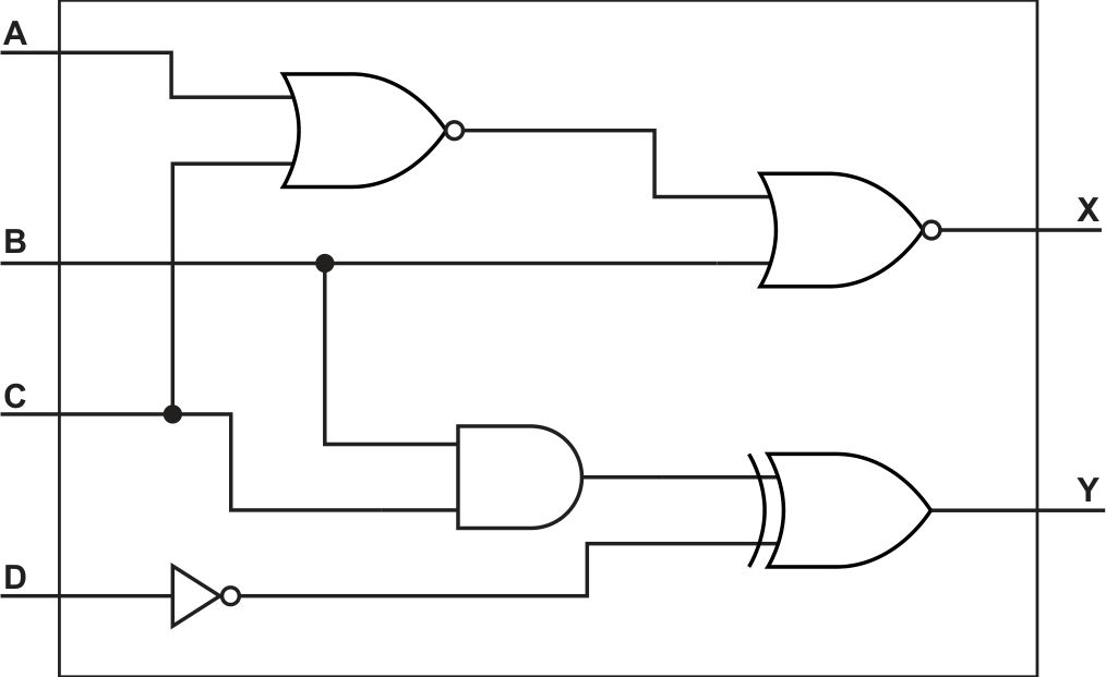
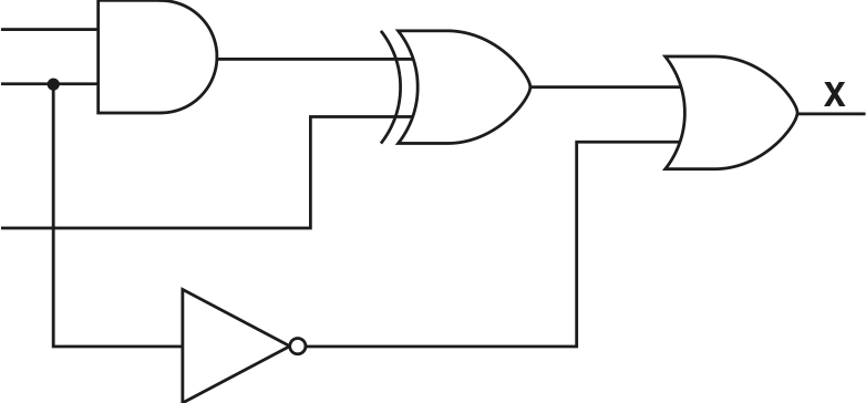
(a) Write the logic expression for the following logic circuit. 3 marks
A
B X
C
(b) Complete the truth table for the following logic expression: 2 marks
X = ( A NAND B ) OR ( A AND NOT C )
| A | B | C | Working space | X |
|---|---|---|---|---|
| 0 | 0 | 0 | ||
| 0 | 0 | 1 | ||
| 0 | 1 | 0 | ||
| 0 | 1 | 1 | ||
| 1 | 0 | 0 | ||
| 1 | 0 | 1 | ||
| 1 | 1 | 0 | ||
| 1 | 1 | 1 |
Show mark scheme
7(a) [3 marks]
1 mark for each section A AND B NOT C AND B // B AND NOT C XOR (with remainder correct and bracketed and nothing extra) X = (A AND B) XOR (NOT C AND B)
7(b) [2 marks]
1 mark for first 4 rows, 1 mark for second 4 rows (shaded) Working space X 0 0 0 1 0 0 1 1 0 1 0 1 0 1 1 1 1 0 0 1 1 0 1 1 1 1 0 1 1 1 1 0
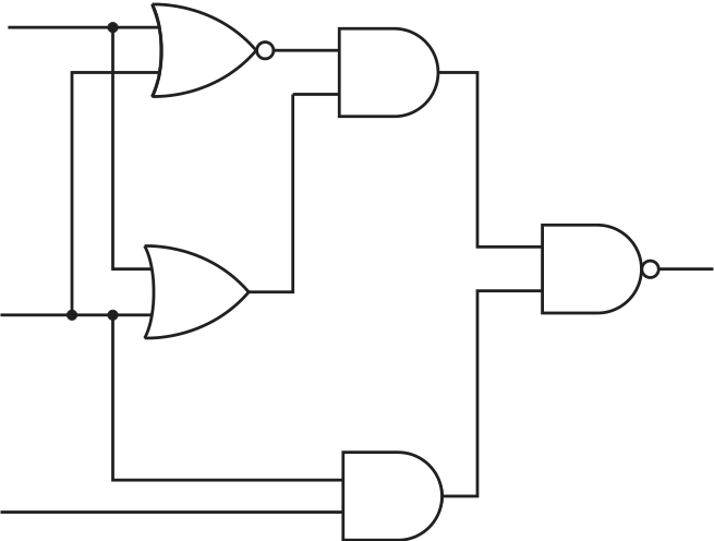
A logic circuit is shown:
A
B
C
(a) Write the logic expression for the logic circuit. 2 marks
 3 marks
| ) Complete | e the truth tab | ble for the g | given logic circuit. | |
|---|---|---|---|---|
| A | B | C | Working space | X |
| 0 | 0 | 0 | ||
| 0 | 0 | 1 | ||
| 0 | 1 | 0 | ||
| 0 | 1 | 1 | ||
| 1 | 0 | 0 | ||
| 1 | 0 | 1 | ||
| 1 | 1 | 0 | ||
| 1 | 1 | 1 |
Show mark scheme
3(a)
1 mark per bullet point A AND B … • … XOR C … • … OR NOT B • ((A AND B) XOR C) OR NOT B
3(b) [2 marks]
1 mark for each set of 4 rows (shaded) Working space X 0 0 0 1 0 0 1 1 0 1 0 0 0 1 1 1 1 0 0 1 1 0 1 1 1 1 0 1 1 1 1 0
3(c) [3 marks]
1 mark for gate, 1 mark for matching symbol, 1 mark for matching truth table NOR OUTPUT 0 0 1 0 1 0 1 0 0 1 1 0 NAND OUTPUT 0 0 1 0 1 1 1 0 1 1 1 0
(a) Complete the truth table for each of the following two logic gates.
A
B
A
B
| A | B | Output |
|---|---|---|
| 0 | 0 | |
| 0 | 1 | |
| 1 | 0 | |
| 1 | 1 |
| A | B | Output |
|---|---|---|
| 0 | 0 | |
| 0 | 1 | |
| 1 | 0 | |
| 1 | 1 |
(b) Draw a logic circuit for the following logic expression. 2 marks 2 marks
X = NOT(NOT( A AND B )AND C ) X A
B
C

Show mark scheme
2(a) [2 marks]
1 mark for each completely correct truth table NOR Output 0 0 1 0 1 0 1 0 0 1 1 0 NAND Output 0 0 1 0 1 1 1 0 1 1 1 0
2(b) [3 marks]
1 mark for each correct bullet point NOT (A AND B) // A NAND B • NOT the result AND C // the result NAND C • OR
A logic circuit is shown:
A
B
C
(a) Write the logic expression for the logic circuit. 2 marks
 3 marks
| ) Complete | e the truth tab | ble for the g | given logic circuit. | |
|---|---|---|---|---|
| A | B | C | Working space | X |
| 0 | 0 | 0 | ||
| 0 | 0 | 1 | ||
| 0 | 1 | 0 | ||
| 0 | 1 | 1 | ||
| 1 | 0 | 0 | ||
| 1 | 0 | 1 | ||
| 1 | 1 | 0 | ||
| 1 | 1 | 1 |
Show mark scheme
3(a)
1 mark per bullet point A AND B … • … XOR C … • … OR NOT B • ((A AND B) XOR C) OR NOT B
3(b) [2 marks]
1 mark for each set of 4 rows (shaded) Working space X 0 0 0 1 0 0 1 1 0 1 0 0 0 1 1 1 1 0 0 1 1 0 1 1 1 1 0 1 1 1 1 0
3(c) [3 marks]
1 mark for gate, 1 mark for matching symbol, 1 mark for matching truth table NOR OUTPUT 0 0 1 0 1 0 1 0 0 1 1 0 NAND OUTPUT 0 0 1 0 1 1 1 0 1 1 1 0
Bobby and Kim are discussing databases.
(a) Bobby tells Kim that a file-based approach is usually better than a relational database. 3 marks
Explain why Bobby is incorrect.
(b) Bobby has a shop that sells products to customers. His database will store data about his customers, their payment details, orders and the products he sells. Customers will have login details to access their accounts. The database will update customers’ payment and login details without keeping any historical records. 3 marks
(i) Give one example of each of the following relationships from Bobby’s database. 1 mark
one-to-one
one-to-many
many-to-many
| dentify the relatio database. | onship that c |
|---|---|
| Relationship | Tick (3) |
| one-to-one | |
| one-to-many | |
| many-to-many |
(iii) Bobby wants to name his database SHOPORDERS . 1 mark
Write a Data Definition Language (DDL) statement to define a new database with the
name SHOPORDERS .
(c) A database has a data dictionary. 3 marks 3 marks
Give three items that are stored in a data dictionary.
1
2
3
| 8 Tick (3) one box in each row to identify the logic | gate that | each state | ement des | scribes. | |
|---|---|---|---|---|---|
| Statement | AND | NAND | NOR | XOR | OR |
| The output is 1 only when both inputs are 1 | |||||
| The output is 1 only when both inputs are different | |||||
| The output is 1 only when both inputs are 0 |
Show mark scheme
7(a) [3 marks]
1 mark per bullet point to max 3 Flat-file has more data redundancy • … because the same data is stored many times // data is stored in • different tables which are linked There is program-data dependence with flat-files • ... because any changes to the structure of the data means the programs • that access that data have to be re-written Flat-file has more data inconsistency // worse data integrity • ... because duplicated data might be stored differently //…because when • data is updated in one place, it is not updated everywhere It is not easy to perform complex searches /queries • … because a new program has to be written each time • Flat files could have a lack of privacy • … as user views cannot easily be implemented •
7(b)(i) [3 marks]
1 mark for each correct example one-to-one e.g. customer to payment details // customer to login details • one-to-many e.g. customer to order • many-to-many e.g. order to product // customer to product •
7(b)(ii) [1 mark]
1 mark Relationship Tick ( ) one-to-one one-to-many many-to-many
7(b)(iii) [1 mark]
1 mark CREATE DATABASE SHOPORDERS;
7(c) [3 marks]
1 mark per item to max 3 table name • field name // attribute • data type • type of validation • Primary Key • Foreign Key • relationships •
A logic expression is given:
Show mark scheme
3(a)
1 mark for each correct gate, with correct inputs
3(b) [2 marks]
1 mark for each half (shaded) Working space S 0 0 0 0 0 0 1 1 0 1 0 1 0 1 1 0 1 0 0 0 1 0 1 1 1 1 0 1 1 1 1 1
Bobby and Kim are discussing databases.
(a) Bobby tells Kim that a file-based approach is usually better than a relational database. 3 marks
Explain why Bobby is incorrect.
(b) Bobby has a shop that sells products to customers. His database will store data about his customers, their payment details, orders and the products he sells. Customers will have login details to access their accounts. The database will update customers’ payment and login details without keeping any historical records. 3 marks
(i) Give one example of each of the following relationships from Bobby’s database. 1 mark
one-to-one
one-to-many
many-to-many
| dentify the relatio database. | onship that c |
|---|---|
| Relationship | Tick (3) |
| one-to-one | |
| one-to-many | |
| many-to-many |
(iii) Bobby wants to name his database SHOPORDERS . 1 mark
Write a Data Definition Language (DDL) statement to define a new database with the
name SHOPORDERS .
(c) A database has a data dictionary. 3 marks 3 marks
Give three items that are stored in a data dictionary.
1
2
3
| 8 Tick (3) one box in each row to identify the logic | gate that | each state | ement des | scribes. | |
|---|---|---|---|---|---|
| Statement | AND | NAND | NOR | XOR | OR |
| The output is 1 only when both inputs are 1 | |||||
| The output is 1 only when both inputs are different | |||||
| The output is 1 only when both inputs are 0 |
Show mark scheme
7(a) [3 marks]
1 mark per bullet point to max 3 Flat-file has more data redundancy • … because the same data is stored many times // data is stored in • different tables which are linked There is program-data dependence with flat-files • ... because any changes to the structure of the data means the programs • that access that data have to be re-written Flat-file has more data inconsistency // worse data integrity • ... because duplicated data might be stored differently //…because when • data is updated in one place, it is not updated everywhere It is not easy to perform complex searches /queries • … because a new program has to be written each time • Flat files could have a lack of privacy • … as user views cannot easily be implemented •
7(b)(i) [3 marks]
1 mark for each correct example one-to-one e.g. customer to payment details // customer to login details • one-to-many e.g. customer to order • many-to-many e.g. order to product // customer to product •
7(b)(ii) [1 mark]
1 mark Relationship Tick ( ) one-to-one one-to-many many-to-many
7(b)(iii) [1 mark]
1 mark CREATE DATABASE SHOPORDERS;
7(c) [3 marks]
1 mark per item to max 3 table name • field name // attribute • data type • type of validation • Primary Key • Foreign Key • relationships •