4.3 Bit Manipulation
AS Level · 17 questions found
What this topic covers
Section titled “What this topic covers”- Binary shifts: logical, arithmetic and cyclic; left and right shift
- Using bit manipulation to monitor/control a device
- Test and set a bit using bit masking
- Bitwise AND, OR, XOR with operand or address; LSL #n, LSR #n
Past paper questions
Section titled “Past paper questions”The table shows part of the instruction set for a processor. The processor has one register, the Accumulator (ACC).
| Instruction | Explanation | |
|---|---|---|
| Opcode | Operand | Operand |
| AND | #n / Bn / &n | Bitwise AND operation of the contents of the ACC with the operand |
| AND | Bitwise AND operation of the contents of the ACC with the contents of |
|
| XOR | #n / Bn / &n | Bitwise XOR operation of the contents of the ACC with the operand |
| XOR | Bitwise XOR operation of the contents of the ACC with the contents of |
|
| OR | #n / Bn / &n | Bitwise OR operation of the contents of the ACC with the operand |
| OR | Bitwise OR operation of the contents of the ACC with the contents of |
|
| LSL | #n | Bits in ACC are shifted logically n places to the left. Zeros are introduced on the right-hand end. |
| LSR | #n | Bits in ACC are shifted logically n places to the right. Zeros are introduced on the left-hand end. |
| can be an absolute or symbolic address # denotes a denary number, e.g. #127 B denotes a binary number, e.g. B10010001 & denotes a hexadecimal number, e.g. &4A |
can be an absolute or symbolic address # denotes a denary number, e.g. #127 B denotes a binary number, e.g. B10010001 & denotes a hexadecimal number, e.g. &4A |
can be an absolute or symbolic address # denotes a denary number, e.g. #127 B denotes a binary number, e.g. B10010001 & denotes a hexadecimal number, e.g. &4A |
(a) The ACC currently contains the following positive binary integer:
0 0 0 1 1 1 1 0
Write a bit manipulation instruction that uses a binary shift to change the contents of the ACC to:
0 1 1 1 1 0 0 0
Instruction [1]
(b) The ACC currently contains the following positive binary integer: 1 mark
1 1 1 0 0 0 1 1
Write the contents of the ACC after the instruction XOR &12 is carried out.
(c) The ACC currently contains the following positive binary integer: 1 mark
1 1 1 0 0 0 1 1
Write the contents of the ACC after the instruction AND #63 is carried out.
(d) The ACC currently contains the following positive binary integer: 1 mark
1 1 1 0 0 0 1 1
The current contents of memory are:
Address Data
98 00100100
99 00110001
100 00110011
101 10100011
102 10101100
Write the contents of the ACC after the instruction OR 100 is carried out.
Show mark scheme
4(a) [1 mark]
1 mark for: LSL #2
4(b) [1 mark]
1 1 1 1 0 0 0 1
4(c) [1 mark]
0 0 1 0 0 0 1 1
4(d) [1 mark]
1 1 1 1 0 0 1 1
(a) The following binary addition is performed using 8‑bit registers.
Complete the calculation using binary addition.
1 0 0 0 0 1 1 1 + 0 0 1 1 1 0 0 1 1 mark
(b) A computer uses the Unicode character set. 1 mark
State the number of bits used to store one character from the Unicode character set.
(c) ASCII is another character set. The ASCII value for the character ‘h’ has the denary value 104.
(i) Write the Binary Coded Decimal (BCD) value for the ASCII character ‘h’. 1 mark
(ii) Write the hexadecimal value for the ASCII character ‘h’. 1 mark
Show mark scheme
7(a) [1 mark]
1 mark for the correct answer 1100 0000
7(b) [1 mark]
1 mark for the correct answer 8 // 16 // 32 // 64
7(c)(i) [1 mark]
1 mark for the correct answer 0001 0000 0100
7(c)(ii) [1 mark]
1 mark for the correct answer 68
The following table shows part of the instruction set for a processor. The processor has two registers: the Accumulator (ACC) and the Index Register (IX).
| Instruction | Explanation | |
|---|---|---|
| Opcode | Operand | Operand |
| LDM | #n | Immediate addressing. Load the number n to the ACC |
| AND | #n / Bn / &n | Bitwise AND operation of the contents of the ACC with the operand |
| AND | Bitwise AND operation of the contents of the ACC with the contents of |
|
| XOR | #n / Bn / &n | Bitwise XOR operation of the contents of the ACC with the operand |
| XOR | Bitwise XOR operation of the contents of the ACC with the contents of |
|
| OR | #n / Bn / &n | Bitwise OR operation of the contents of the ACC with the operand |
| OR | Bitwise OR operation of the contents of the ACC with the contents of |
|
| CMP | #n | Compare the contents of the ACC with number n |
| CMP | Compare the contents of the ACC with the contents of | |
| LSL | #n | Bits in the ACC are shifted logically n places to the left. Zeros are introduced on the right‑hand end |
| LSR | #n | Bits in the ACC are shifted logically n places to the right. Zeros are introduced on the left‑hand end |
| can be an absolute or symbolic address # denotes a denary number, e.g. #127 B denotes a binary number, e.g. B10010001 & denotes a hexadecimal number, e.g. &4A |
can be an absolute or symbolic address # denotes a denary number, e.g. #127 B denotes a binary number, e.g. B10010001 & denotes a hexadecimal number, e.g. &4A |
can be an absolute or symbolic address # denotes a denary number, e.g. #127 B denotes a binary number, e.g. B10010001 & denotes a hexadecimal number, e.g. &4A |
The current contents of main memory are shown:
Address Data
100 0000 0011
101 1010 1110
102 1100 1100
103 1111 1111
104 1100 1100
(a) Complete the table by writing the contents of the ACC after the execution of each instruction. 4 marks
| Current contents of the ACC |
Instruction | Contents of the ACC after the execution of the instruction |
|---|---|---|
| 0000 1111 | AND 101 | |
| 0000 0000 | LDM #100 | |
| 0000 0001 | XOR &F1 | |
| 0001 0001 | CMP 101 |
(b) The Von Neumann model for a computer system uses registers. 4 marks
Describe the role of the Memory Address Register (MAR) and Memory Data Register (MDR) in the fetch‑execute (F‑E) cycle.
(c) Assembly language instructions are grouped. 3 marks
Complete each statement by writing the name of the appropriate instruction group.
Loading data into the accumulator is an example of an instruction in the
______ group. Incrementing the index register is an example
of an instruction in the ______ group. Branching to another
address is an example of an instruction in the ______ group.
Show mark scheme
6(a) [4 marks]
1 mark for each correct row Current contents Instruction Contents of the ACC of the ACC after the execution of the instruction 0000 1111 AND 101 0000 1110 0000 0000 LDM #100 0110 0100 0000 0001 XOR &F1 1111 0000 0001 0001 CMP 101 0001 0001
6(b) [4 marks]
1 mark for each bullet point, max 4 marks • MAR stores the address of the next instruction / data to be read from / or written to memory • The address is received from the Program Counter (PC) • The MDR stores the data / instruction in the address stored in the MAR which has been read / written • The instruction passes to the CIR for decoding and executing
6(c) [3 marks]
1 mark for each bullet point, max 3 marks • Data movement • Arithmetic operations • Conditional and unconditional (jump) instructions
(a) A computer can perform logical and arithmetic shifts.
(i) Show the result of a logical left shift of 2 places on the two’s complement binary integer 11001010 1 mark
(ii) Show the result of an arithmetic right shift of 3 places on the two’s complement binary integer 10011110 1 mark
(b) Complete the following binary addition. Show your working. Include any overflow bit(s).
1 1 1 1 0 1 0 1 + 1 0 1 1 0 0 0 1 1 mark
(c) Subtract the binary number 00011110 from the binary number 01100100 using binary subtraction. Show your working. 2 marks
Show mark scheme
7(a)(i) [1 mark]
1 mark for 0010 1000
7(a)(ii) [1 mark]
1 mark for 1111 0011
7(b) [1 mark]
1 mark for 1 1 1 1 0 1 0 1 + 1 0 1 1 0 0 0 1 1 1 1 1 1 (1) 1 0 1 0 0 1 1 0 Answer: (1) 1010 0110
7(c) [2 marks]
1 mark for showing binary subtraction (any method) Direct subtraction: 1 1 1 1 0 1 1 0 0 1 0 0 -0 0 0 1 1 1 1 0 1 1 1 1 0 1 0 0 0 1 1 0 Adding the two’s complement: 0 1 1 0 0 1 0 0 + 1 1 1 0 0 0 1 0 1 1 1 (1) 0 1 0 0 0 1 1 0 1 mark for answer 0100 0110
(a) Convert the hexadecimal number 1FAB into denary.
Working
Denary value [1]
(b) Explain how to convert the two’s complement integer 10011111 into denary. Give the denary value after conversion. 3 marks
Explanation
Denary value
(c) Describe the difference between a right logical binary shift and a right arithmetic binary shift. 2 marks
Show mark scheme
8(a) [1 mark]
1 mark for: Denary value: 8107
8(b) [3 marks]
1 mark for each bullet point for the method ( max 2 ) e.g. • Flip each bit then add 1 … • … method of converting the new binary number into denary • Most significant 1 bit is treated as the corresponding negative denary value … • … add the other positive corresponding denary values 1 mark for correct conversion Denary value: −97
8(c) [2 marks]
1 mark each: • A logical shift moves all bits to the right and inserts zeros in the appropriate leftmost bits • An arithmetic shift moves all bits to the right but copies the sign bit into the Most Significant Bit (MSB)
The following table shows part of the instruction set for a processor. The processor has two registers: the Accumulator (ACC) and an Index Register (IX).
| Instruction | Explanation | |
|---|---|---|
| Opcode | Operand | Operand |
LDM |
#n |
Immediate addressing. Load the number n to ACC |
LDD |
<address> |
Direct addressing. Load the contents of the location at the given address to ACC |
LDI |
<address> |
Indirect addressing. The address to be used is at the given address. Load the contents of this second address to ACC |
LDX |
<address> |
Indexed addressing. Form the address from + the contents of the Index Register. Copy the contents of this calculated address to ACC |
LDR |
#n |
Immediate addressing. Load the number n to IX |
ADD |
#n/Bn/&n |
Add the number n to the ACC |
ADD |
<address> |
Add the contents of the given address to the ACC |
SUB |
#n/Bn/&n |
Subtract the number n from the ACC |
SUB |
<address> |
Subtract the contents of the given address from the ACC |
INC |
<register> |
Add 1 to the contents of the register (ACC or IX) |
| can be an absolute or a symbolic address # denotes a denary number, e.g. #123 B denotes a binary number, e.g. B01001010 & denotes a hexadecimal number, e.g. &4A |
can be an absolute or a symbolic address # denotes a denary number, e.g. #123 B denotes a binary number, e.g. B01001010 & denotes a hexadecimal number, e.g. &4A |
can be an absolute or a symbolic address # denotes a denary number, e.g. #123 B denotes a binary number, e.g. B01001010 & denotes a hexadecimal number, e.g. &4A |
(a) The current contents of memory are shown: 4 marks 3 marks
Address Data
19 24
20 2
21 1
22 3
23 5
24 4
25 22
The current contents of the ACC and IX are shown:
ACC 12
IX 1
Complete the table by writing the content of the ACC after each program has run.
| Program number | Code | ACC content |
|---|---|---|
| 1 | LDD 20ADD #2 |
|
| 2 | LDX 22 |
|
| 3 | LDI 25INC ACCSUB 22 |
|
| 4 | LDD 19LDM #5LDM #25 |
|
| (b) The processor incl | ludes these bit manipulation instructions: | |
| --- | --- | --- |
| Instruction | Instruction | Explanation |
| Opcode | Operand | Operand |
AND |
#n/Bn/&n |
Bitwise AND operation of the contents of ACC with the operand |
AND |
<address> |
Bitwise AND operation of the contents of ACC with the contents of |
XOR |
#n/Bn/&n |
Bitwise XOR operation of the contents of ACC with the operand |
XOR |
<address> |
Bitwise XOR operation of the contents of ACC with the contents of |
OR |
#n/Bn/&n |
Bitwise OR operation of the contents of ACC with the operand |
OR |
<address> |
Bitwise OR operation of the contents of ACC with the contents of |
| can be an absolute or a symbolic address # denotes a denary number, e.g. #123 B denotes a binary number, e.g. B01001010 & denotes a hexadecimal number, e.g. &4A |
can be an absolute or a symbolic address # denotes a denary number, e.g. #123 B denotes a binary number, e.g. B01001010 & denotes a hexadecimal number, e.g. &4A |
can be an absolute or a symbolic address # denotes a denary number, e.g. #123 B denotes a binary number, e.g. B01001010 & denotes a hexadecimal number, e.g. &4A |
The current contents of memory are shown:
Address Data
        30 01110101
        31 11111111
        32 00000000
        33 11001100
        34 10101010
The current content of the ACC is shown:
1 0 0 1 1 0 1 0
Complete the table by writing the content of the ACC after each program has run.
The binary number 10011010 is reloaded into the ACC before each program is run.
| Program number | Code | ACC content |
|---|---|---|
| 1 | AND 31 |
|
| 2 | XOR B01001111 |
|
| 3 | OR #30 |
Show mark scheme
4(a) [4 marks]
1 mark for each correct answer: Program Code ACC Number Content LDD 20 1 4 ADD #2 LDX 22 2 5 LDI 25 3 1 INC ACC SUB 22 LDD 19 4 25 LDM #5 LDM #25
4(b) [3 marks]
1 mark for each correct answer: Program Code ACC Content Number AND 31 1 1001 1010 XOR B01001111 2 1101 0101 OR #30 3 1001 1110
The following table shows part of the instruction set for a processor. The processor has two registers: the Accumulator (ACC) and an Index Register (IX).
| Instruction | Explanation | |
|---|---|---|
| Opcode | Operand | Operand |
LDM |
#n |
Immediate addressing. Load the number n to ACC |
LDD |
<address> |
Direct addressing. Load the contents of the location at the given address to ACC |
LDI |
<address> |
Indirect addressing. The address to be used is at the given address. Load the contents of this second address to ACC |
LDX |
<address> |
Indexed addressing. Form the address from + the contents of the index register. Copy the contents of this calculated address to ACC |
LDR |
#n |
Immediate addressing. Load the number n to IX |
ADD |
#n/Bn/&n |
Add the number n to the ACC |
ADD |
<address> |
Add the contents of the given address to the ACC |
SUB |
#n/Bn/&n |
Subtract the number n from the ACC |
SUB |
<address> |
Subtract the contents of the given address from the ACC |
INC |
<register> |
Add 1 to the contents of the register (ACC or IX) |
| can be an absolute or a symbolic address # denotes a denary number, e.g. #123 B denotes a binary number, e.g. B01001010 & denotes a hexadecimal number, e.g. &4A |
can be an absolute or a symbolic address # denotes a denary number, e.g. #123 B denotes a binary number, e.g. B01001010 & denotes a hexadecimal number, e.g. &4A |
can be an absolute or a symbolic address # denotes a denary number, e.g. #123 B denotes a binary number, e.g. B01001010 & denotes a hexadecimal number, e.g. &4A |
(a) The current contents of memory are shown: 4 marks 3 marks
Address Data
10 1
11 3
12 5
13 11
14 10
15 16
16 12
The current contents of the ACC and IX are shown:
ACC 10
IX 0
Complete the table by writing the content of the ACC after each program has run.
| Program number | Code | ACC content |
|---|---|---|
| 1 | LDI 15SUB #1 |
|
| 2 | LDD 14ADD 11 |
|
| 3 | LDM #11ADD #3SUB 16 |
|
| 4 | LDR #2LDX 14ADD #2 |
|
| (b) The processor inclu | udes these bit manipulation instructions: | |
| --- | --- | --- |
| Instruction | Instruction | Explanation |
| Opcode | Operand | Operand |
AND |
#n/Bn/&n |
Bitwise AND operation of the contents of ACC with the operand |
AND |
<address> |
Bitwise AND operation of the contents of ACC with the contents of |
XOR |
#n/Bn/&n |
Bitwise XOR operation of the contents of ACC with the operand |
XOR |
<address> |
Bitwise XOR operation of the contents of ACC with the contents of |
OR |
#n/Bn/&n |
Bitwise OR operation of the contents of ACC with the operand |
OR |
<address> |
Bitwise OR operation of the contents of ACC with the contents of |
| can be an absolute or a symbolic address # denotes a denary number, e.g. #123 B denotes a binary number, e.g. B01001010 & denotes a hexadecimal number, e.g. &4A |
can be an absolute or a symbolic address # denotes a denary number, e.g. #123 B denotes a binary number, e.g. B01001010 & denotes a hexadecimal number, e.g. &4A |
can be an absolute or a symbolic address # denotes a denary number, e.g. #123 B denotes a binary number, e.g. B01001010 & denotes a hexadecimal number, e.g. &4A |
The current contents of memory are shown:
Address Data
25 11000110
26 11100001
27 10000001
28 11001101
29 00001111
The current content of the ACC is shown:
0 1 0 0 0 1 1 0
Complete the table by writing the content of the ACC after each program has run.
The binary number 01000110 is reloaded into the ACC before each program is run.
| Program number | Code | ACC content |
|---|---|---|
| 1 | XOR 29 |
|
| 2 | AND #29 |
|
| 3 | OR B11111111 |
Show mark scheme
5(a) [4 marks]
1 mark for each correct answer: Program Code ACC Content Number 1 LDI 15 11 SUB #1 2 LDD 14 13 ADD 11 2 3 LDM #11 ADD #3 SUB 16 4 LDR #2 14 LDX 14 ADD #2
5(b) [3 marks]
1 mark for each correct answer: Program Code ACC Content Number 1 XOR 29 0100 1001 2 AND #29 0000 0100 3 OR B11111111 1111 1111
(a) Identify the purpose of the first pass of a two-pass assembler. 1 mark
(b) The following table shows part of the instruction set for a processor. The processor has two registers, the Accumulator (ACC) and the Index Register (IX).
| Instruction | Explanation | |
|---|---|---|
| Opcode | Operand | Operand |
LDR |
#n |
Immediate addressing. Load the number n to IX |
STO |
<address> |
Store contents of ACC at the given address |
ADD |
<address> |
Add the contents of the given address to the ACC |
INC |
<register> |
Add 1 to the contents of the register (ACC or IX) |
CMP |
#n |
Compare the contents of ACC with number n |
JPE |
<address> |
Following a compare instruction, jump to if the compare was True |
OUT |
Output to the screen the character whose ASCII value is stored in ACC | |
| can be an absolute or symbolic address # denotes a denary number, e.g. #123 |
can be an absolute or symbolic address # denotes a denary number, e.g. #123 |
can be an absolute or symbolic address # denotes a denary number, e.g. #123 |
(i) Give one example of an instruction that belongs to each of the following instruction groups. 3 marks
Only use the instructions given in the table. Each instruction must have a suitable operand.
Data movement
Arithmetic operation
Conditional instruction
(ii) The instruction LDR #2 uses immediate addressing. 2 marks
Give one similarity and one difference between direct addressing and indexed addressing.
Similarity
Difference
(iii) Identify one other mode of addressing. 1 mark
(c) The following table shows another part of the instruction set for the same processor.
| Instruction | Explanation | |
|---|---|---|
| Opcode | Operand | Operand |
AND |
Bn |
Bitwise AND operation of the contents of ACC with the operand |
XOR |
Bn |
Bitwise XOR operation of the contents of ACC with the operand |
LSR |
#n |
Bits in ACC are shifted logically n places to the right. Zeros are introduced on the left hand end |
| # denotes a denary number, e.g. #123 B denotes a binary number, e.g. B01001101 |
# denotes a denary number, e.g. #123 B denotes a binary number, e.g. B01001101 |
# denotes a denary number, e.g. #123 B denotes a binary number, e.g. B01001101 |
(i) The current contents of the ACC are: 1 mark
0 1 0 0 1 1 1 1
Show the contents of the ACC after the execution of the following instruction.
AND B10100101
(ii) The current contents of the ACC are: 1 mark
0 0 0 1 0 1 1 1
Show the contents of the ACC after the execution of the following instruction.
LSR #3
(iii) The current contents of the ACC are: 1 mark
1 1 1 1 0 1 1 1
Show the contents of the ACC after the execution of the following instruction.
XOR B00100101
Show mark scheme
8(a) [1 mark]
1 mark for: • To create a symbol table
8(b)(i) [3 marks]
1 mark for each bullet point • Data movement: e.g. LDR #50 // STO 201 • Arithmetic operation: e.g. ADD 100 // INC IX • Conditional instruction: e.g. JPE 96
8(b)(ii) [2 marks]
1 mark for each bullet point ( max 2 ) Similarity: • both load the contents of an address into the Accumulator Difference: • direct accesses the address given by the operand whereas indexed adds the contents of IX to the operand and accesses the data at that calculated address
8(b)(iii) [1 mark]
1 mark for • Indirect (addressing) • Relative (addressing)
8(c)(i) [1 mark]
0000 0101
8(c)(ii) [1 mark]
0000 0010
8(c)(iii) [1 mark]
1101 0010
A computer has an Operating System (OS).
(a) Describe how the Operating System manages the peripheral hardware devices of the computer. 4 marks
(b) Hardware management is one key management task carried out by the Operating System. 2 marks
Identify two other key management tasks carried out by the Operating System.
1
2
(c) The Operating System has utility software including defragmentation software. 3 marks
Explain how defragmentation can improve the performance of the computer.
(d) The computer stores data in binary form.
(i) State the difference between a kibibyte and a kilobyte. 1 mark
(ii) Convert the denary number 964 into Binary Coded Decimal (BCD). 1 mark
(iii) Convert the positive binary integer 11110010 into hexadecimal. 1 mark
(iv) Give the smallest and largest two’s complement binary number that can be represented using 8 bits. 2 marks
Smallest
Largest
(v) Add the following two binary integers using binary addition. Show your working. 2 marks
1 0 1 1 0 0 0 0 + 0 0 0 1 1 0 1 1
(vi) Show the result of a 3‑place right logical shift on the binary number: 1 mark
11001100
Show mark scheme
3(a) [4 marks]
1 mark each to max 4 Examples: Installs device drivers … to allow communication between peripherals and computer Sends data and receives data to and from peripherals … such as to an output device and from an input device/by example Handles buffers for transfer of data … to ensure smooth transfer between devices that transmit and receive at different speeds Manages interrupts / signals from the device
3(b) [2 marks]
1 mark each to max 2 Memory management File management Security management Process management Error checking and recovery
3(c) [1 mark]
1 mark each to max 3 Rearranges blocks of individual files (on the HDD) so they are contiguous // moves the free space together Accessing each file is faster …because there is no need to search for the next fragment / block of the file …so less head movement is needed
3(d)(i)
1 mark from Kibibyte is 1024 bytes and kilobyte is 1000 bytes Kibibyte is binary prefix and kilobyte is denary prefix
3(d)(ii) [1 mark]
1001 0110 0100
3(d)(iii) [1 mark]
F2
3(d)(iv) [2 marks]
Smallest: 10000000 Largest: 01111111
3(d)(v)
1 mark for working 1 mark for answer 1 0 1 1 0 0 0 0
- 0 0 0 1 1 0 1 1 1 1 0 0 1 0 1 1 1 1
3(d)(vi) [2 marks]
00011001
Data in a computer is stored in binary form.
(a) State the number of unique binary values that can be represented in 16 bits. 1 mark
(b) Give the 8‑bit one’s complement representation of the denary number −120. 2 marks
Show your working.
Working
Answer
(c) Convert the hexadecimal number A04 into denary. 2 marks
Show your working.
Working
Answer
(d) Show the result of a 2‑place left logical shift on the binary number: 1 mark
01001111
Show mark scheme
4(a) [2 marks]
2 // 65536 16
4(b)
1 mark for working; 1 mark for answer Working: +120 = 0111 1000 Answer: 1000 0111
4(c) [2 marks]
1 mark for working; 1 mark for answer ) + 4 Working: A04 = (10 * 16 2 // A04 = (10 * 256) + 4 // A04 = 1010 0000 0100 Answer: 2564
4(d) [1 mark]
0011 1100
(a) A computer system is designed using the basic Von Neumann model.
(i) Describe the role of the registers in the Fetch-Execute (F-E) cycle. 5 marks
(ii) Describe when interrupts are detected in the F-E cycle and how the interrupts are handled. 5 marks
Detected
Handled
(b) Identify one factor that can affect the performance of the computer system and state how it impacts the performance. 2 marks
Factor
Impact Question 6 continues on the next page.
(c) The table shows part of the instruction set for a processor. The processor has one general purpose register, the Accumulator (ACC).
| Instruction | Explanation | |
|---|---|---|
| Opcode | Operand | Operand |
AND |
#n |
Bitwise AND operation of the contents of ACC with the operand |
XOR |
#n |
Bitwise XOR operation of the contents of ACC with the operand |
OR |
#n |
Bitwise OR operation of the contents of ACC with the operand |
LSL |
#n |
Bits in ACC are shifted logically n places to the left. Zeros are introduced on the right hand end |
LSR |
#n |
Bits in ACC are shifted logically n places to the right. Zeros are introduced on the left hand end |
| # denotes a denary number, e.g. #123 | # denotes a denary number, e.g. #123 | # denotes a denary number, e.g. #123 |
(i) Complete the register to show the result after the instruction AND #2 is executed. 1 mark
Register before: 0 1 1 0 1 1 0 1
Register after:
(ii) Complete the register to show the result after the instruction OR #8 is executed. 1 mark
Register before: 0 1 1 0 1 1 0 1
Register after:
(iii) Complete the register to show the result after the operation LSL #4 is executed. 1 mark
Register before: 0 1 1 0 1 1 0 1
Register after:
Show mark scheme
6(a)(i) [5 marks]
1 mark per bullet point to max 5 The Program Counter (PC) holds the address of the next instruction … …and the contents are incremented / changed to the next address each cycle The Memory Address Register (MAR) holds the address to fetch the data (from the PC) The Memory Data Register (MDR) holds the data at the address in MAR The instruction is transferred to Current Instruction Register (CIR) for decoding and execution
6(a)(ii) [5 marks]
1 mark for detection At the start/end of a FE cycle 1 mark for handling to max 4 Priority is checked If lower priority than current process continue with F-E cycle If higher priority than current process … … state of current process is / registers are stored on stack Location / type of interrupt identified... …appropriate ISR is called to handle the interrupt When ISR finished, check for further interrupts (of high priority) / return to step 1 Otherwise load data from stack and continue with process
6(b) [2 marks]
1 mark for factor 1 mark for impact e.g. Clock speed… …higher clock speed means more FE cycles per second Number of cores… …means more instructions can be carried out simultaneously Bus width … …allows the transfer of more data each time // allows more memory locations to be directly accessed Cache … … the higher capacity the more frequently used instructions it can store for fast access
6(c)(i) [1 mark]
0000 0000
6(c)(ii) [1 mark]
0110 1101
6(c)(iii) [1 mark]
1101 0000
The table shows part of the instruction set for a processor. The processor has one general purpose register, the Accumulator (ACC).
| Instruction | Explanation | |
|---|---|---|
| Opcode | Operand | Operand |
AND |
#n |
Bitwise AND operation of the contents of ACC with the operand |
AND |
<address> |
Bitwise AND operation of the contents of ACC with the contents of |
XOR |
#n |
Bitwise XOR operation of the contents of ACC with the operand |
XOR |
<address> |
Bitwise XOR operation of the contents of ACC with the contents of |
OR |
#n |
Bitwise OR operation of the contents of ACC with the operand |
OR |
<address> |
Bitwise OR operation of the contents of ACC with the contents of |
| can be an absolute or a symbolic address # denotes a denary number, e.g. #123 |
can be an absolute or a symbolic address # denotes a denary number, e.g. #123 |
can be an absolute or a symbolic address # denotes a denary number, e.g. #123 |
(a) The ACC currently contains the following positive binary integer: 2 marks
0 1 1 0 0 1 0 1
Write the bit manipulation instruction that would change the binary integer in ACC to:
1 1 1 1 1 1 1 1
Opcode ______ Operand
(b) The ACC currently contains the following positive binary integer: 2 marks
0 1 1 0 0 1 0 1
Write the bit manipulation instruction that would change the binary integer in ACC to:
1 0 0 1 1 0 1 0
Opcode ______ Operand
Show mark scheme
3(a) [2 marks]
1 mark for correct opcode and 1 mark for corresponding operand OR #255 // OR #154 // XOR #154 e.g. OR... ... #255
3(b) [2 marks]
1 mark for correct opcode and 1 mark for corresponding operand XOR #255 e.g. XOR... ... #255
3(c) [1 mark]
7E
3(d) [1 mark]
11110000
3(e) [2 marks]
1 mark per point Correct conversion to binary 01111111 (127) and 00001100 (12) Working e.g. turning 01111111 into two's complement 10000001 Answer: 1000 1101
(a) There are two errors in the following register transfer notation for the fetch‑execute cycle. 4 marks
1 MAR [PC]
2 PC [PC] − 1
      3 MDR  [MAR]
      4 CIR  [MDR]
Complete the following table by:
identifying the line number of each error
describing the error
writing the correct statement.
Line
numberDescription of the error Correct statement
(b) The following table shows part of the instruction set for a processor. The processor has one general purpose register, the Accumulator (ACC), and an Index Register (IX). 4 marks
| Instruction | Explanation | |
|---|---|---|
| Opcode | Operand | Operand |
LDM |
#n |
Immediate addressing. Load the number n to ACC |
LDD |
<address> |
Direct addressing. Load the contents of the location at the given address to ACC |
STO |
<address> |
Store the contents of ACC at the given address |
INC |
<register> |
Add 1 to the contents of the register (ACC or IX) |
CMP |
<address> |
Compare the contents of ACC with the contents of |
JPN |
<address> |
Following a compare instruction, jump to if the compare was False |
JMP |
<address> |
Jump to the given address |
IN |
Key in a character and store its ASCII value in ACC | |
OUT |
Output to the screen the character whose ASCII value is stored in ACC | |
END |
Return control to the operating system | |
XOR |
#n |
Bitwise XOR operation of the contents of ACC with the operand |
XOR |
<address> |
Bitwise XOR operation of the contents of ACC with the contents of |
AND |
#n |
Bitwise AND operation of the contents of ACC with the operand |
AND |
<address> |
Bitwise AND operation of the contents of ACC with the contents of |
OR |
#n |
Bitwise OR operation of the contents of ACC with the operand |
OR |
<address> |
Bitwise OR operation of the contents of ACC with the contents of |
LSL |
#n |
Bits in ACC are shifted logically n places to the left. Zeros are introduced on the right hand end |
LSR |
#n |
Bits in ACC are shifted logically n places to the right. Zeros are introduced on the left hand end |
| can be an absolute or symbolic address # denotes a denary number, e.g. #123 B denotes a binary number, e.g. B01001101 |
can be an absolute or symbolic address # denotes a denary number, e.g. #123 B denotes a binary number, e.g. B01001101 |
can be an absolute or symbolic address # denotes a denary number, e.g. #123 B denotes a binary number, e.g. B01001101 |
The current contents of main memory are shown:
Address Data
        100 00001111
        101 11110000
        102 01010101
        103 11111111
        104 00000000
Each row of the following table shows the current contents of ACC in binary and the instruction that will be performed on those contents.
| Complete the table by w instruction. | writing the new contents of the A | ACC after the execution of each |
|---|---|---|
| Current contents of the ACC | Instruction | New contents of the ACC |
11111111 |
OR 101 |
|
00000000 |
XOR #15 |
|
10101010 |
LSR #2 |
|
01010101 |
AND 104 |
Show mark scheme
6(a) [4 marks]
1 mark for identification of line and description of error 1 mark for the correct statement Line Description of the error Correct statement number 2 Program Counter should be incremented, ← PC [PC] + 1 not decremented 3 It should be the contents of the address in ← MDR [[MAR]] the MAR
6(b) [2 marks]
1 mark for each correct row Current contents of the ACC Instruction New contents of the ACC 11111111 OR 101 11111111 00000000 XOR #15 00001111 10101010 LSR #2 00101010 01010101 AND 104 00000000
The Von Neumann model for a computer system uses registers.
(a) Describe the role of the following special purpose registers in the fetch-execute (F-E) cycle.
(i) Memory Address Register (MAR) 4 marks
Memory Data Register (MDR)
(ii) Another special purpose register is the Index Register. 1 mark
Identify one other special purpose register used in the Von Neumann model for a computer system.
(b) The following table shows part of the instruction set for a processor. The processor has one general purpose register, the Accumulator (ACC), and an Index Register (IX).
| Instruction | Explanation | |
|---|---|---|
| Opcode | Operand | Operand |
LDM |
#n |
Immediate addressing. Load the number n to ACC |
LDD |
<address> |
Direct addressing. Load the contents of the location at the given address to ACC |
STO |
<address> |
Store the contents of ACC at the given address |
INC |
<register> |
Add 1 to the contents of the register (ACC or IX) |
CMP |
<address> |
Compare the contents of ACC with the contents of |
JPN |
<address> |
Following a compare instruction, jump to if the compare was False |
JMP |
<address> |
Jump to the given address |
IN |
Key in a character and store its ASCII value in ACC | |
OUT |
Output to the screen the character whose ASCII value is stored in ACC | |
END |
Return control to the operating system | |
XOR |
#n |
Bitwise XOR operation of the contents of ACC with the operand |
XOR |
<address> |
Bitwise XOR operation of the contents of ACC with the contents of |
OR |
#n |
Bitwise OR operation of the contents of ACC with the operand |
OR |
<address> |
Bitwise OR operation of the contents of ACC with the contents of |
AND |
#n |
Bitwise AND operation of the contents of ACC with the operand |
AND |
<address> |
Bitwise AND operation of the contents of ACC with the contents of |
LSL |
#n |
Bits in ACC are shifted logically n places to the left. Zeros are introduced on the right hand end |
LSR |
#n |
Bits in ACC are shifted logically n places to the right. Zeros are introduced on the left hand end |
| can be an absolute or symbolic address # denotes a denary number, e.g. #123 |
can be an absolute or symbolic address # denotes a denary number, e.g. #123 |
can be an absolute or symbolic address # denotes a denary number, e.g. #123 |
The current contents of main memory are shown:
Address Data
        100 01010101
        101 11110000
        102 00001111
        103 00000000
        104 11111111
(i) In the following table, each row shows the current contents of the ACC in binary and the instruction that will be performed on those contents. 4 marks
| Complete the table instruction. | by writing the new contents of the | e ACC after the execution of each |
|---|---|---|
| Current contents of the ACC | Instruction | New contents of the ACC |
01010101 |
XOR 101 |
|
11110000 |
AND 104 |
|
00001111 |
LSL #4 |
|
11111111 |
OR 102 |
(ii) The following table contains five assembly language instruction groups. 4 marks
Write an appropriate assembly language instruction for each instruction group, using the given instruction set. The first one has been completed for you.
| Instruction Group | Instruction |
|---|---|
| Data movement | LDM #2 |
| Input and output of data | |
| Arithmetic operations | |
| Unconditional and conditional instructions | |
| Compare instructions |
(iii) The opcode LDM uses immediate addressing. The opcode LDD uses direct addressing. 2 marks
Identify and describe one additional mode of addressing.
Mode of addressing
Description
Show mark scheme
8(a)(i) [1 mark]
1 mark for each bullet point to max 2 for each register MAR Stores the next address to be fetched • ... held in the Program Counter (PC) • The data at this address is then fetched • MDR Stores the data from the address pointed to by the MAR • The data in it is copied to the Current Instruction Register (CIR) •
8(a)(ii)
1 mark for a correct register e.g. Program Counter (PC) Current Instruction Register (CIR) Status register Interrupt register
8(b)(i) [4 marks]
1 mark for each correct answer Current contents of New contents of Instruction the ACC the ACC 01010101 XOR 101 1010 0101 11110000 AND 104 1111 0000 00001111 LSL #4 1111 0000 11111111 OR 102 1111 1111
8(b)(ii) [4 marks]
1 mark for each correct instruction Instruction Group Instruction Data movement LDM #2 Input and output of data IN / OUT Arithmetic Operations INC ACC / INC IX Unconditional and conditional instructions JPN 100 / JMP 100 Compare instructions CMP 100
8(b)(iii) [2 marks]
1 mark for name, 1 mark for description Indirect addressing • the address to be used is at the given address • Relative addressing • the address to be used is an offset number of locations away, relative to • the address of the current instruction Indexed addressing • form the address from the given address plus the contents of the index • register
(a) There are two errors in the following register transfer notation for the fetch‑execute cycle. 4 marks
1 MAR [PC]
2 PC [PC] − 1
      3 MDR  [MAR]
      4 CIR  [MDR]
Complete the following table by:
identifying the line number of each error
describing the error
writing the correct statement.
Line
numberDescription of the error Correct statement
(b) The following table shows part of the instruction set for a processor. The processor has one general purpose register, the Accumulator (ACC), and an Index Register (IX). 4 marks
| Instruction | Explanation | |
|---|---|---|
| Opcode | Operand | Operand |
LDM |
#n |
Immediate addressing. Load the number n to ACC |
LDD |
<address> |
Direct addressing. Load the contents of the location at the given address to ACC |
STO |
<address> |
Store the contents of ACC at the given address |
INC |
<register> |
Add 1 to the contents of the register (ACC or IX) |
CMP |
<address> |
Compare the contents of ACC with the contents of |
JPN |
<address> |
Following a compare instruction, jump to if the compare was False |
JMP |
<address> |
Jump to the given address |
IN |
Key in a character and store its ASCII value in ACC | |
OUT |
Output to the screen the character whose ASCII value is stored in ACC | |
END |
Return control to the operating system | |
XOR |
#n |
Bitwise XOR operation of the contents of ACC with the operand |
XOR |
<address> |
Bitwise XOR operation of the contents of ACC with the contents of |
AND |
#n |
Bitwise AND operation of the contents of ACC with the operand |
AND |
<address> |
Bitwise AND operation of the contents of ACC with the contents of |
OR |
#n |
Bitwise OR operation of the contents of ACC with the operand |
OR |
<address> |
Bitwise OR operation of the contents of ACC with the contents of |
LSL |
#n |
Bits in ACC are shifted logically n places to the left. Zeros are introduced on the right hand end |
LSR |
#n |
Bits in ACC are shifted logically n places to the right. Zeros are introduced on the left hand end |
| can be an absolute or symbolic address # denotes a denary number, e.g. #123 B denotes a binary number, e.g. B01001101 |
can be an absolute or symbolic address # denotes a denary number, e.g. #123 B denotes a binary number, e.g. B01001101 |
can be an absolute or symbolic address # denotes a denary number, e.g. #123 B denotes a binary number, e.g. B01001101 |
The current contents of main memory are shown:
Address Data
        100 00001111
        101 11110000
        102 01010101
        103 11111111
        104 00000000
Each row of the following table shows the current contents of ACC in binary and the instruction that will be performed on those contents.
| Complete the table by w instruction. | writing the new contents of the A | ACC after the execution of each |
|---|---|---|
| Current contents of the ACC | Instruction | New contents of the ACC |
11111111 |
OR 101 |
|
00000000 |
XOR #15 |
|
10101010 |
LSR #2 |
|
01010101 |
AND 104 |
Show mark scheme
6(a) [4 marks]
1 mark for identification of line and description of error 1 mark for the correct statement Line Description of the error Correct statement number 2 Program Counter should be incremented, ← PC [PC] + 1 not decremented 3 It should be the contents of the address in ← MDR [[MAR]] the MAR
6(b) [2 marks]
1 mark for each correct row Current contents of the ACC Instruction New contents of the ACC 11111111 OR 101 11111111 00000000 XOR #15 00001111 10101010 LSR #2 00101010 01010101 AND 104 00000000
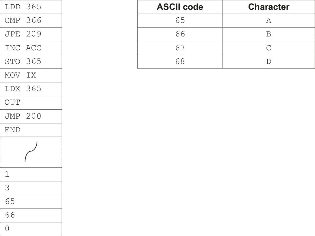
The current contents of the main memory and selected values from the ASCII character set are shown.
Address Instruction ASCII code table (selected codes only)

| ASCII code | Character |
|---|---|
65 |
A |
66 |
B |
67 |
C |
68 |
D |
…
Complete the trace table for the program currently in main memory. 6 marks
| Instruction address |
ACC | Memory address | IX | Output | |||
|---|---|---|---|---|---|---|---|
| Instruction address |
ACC | 365 |
366 |
367 |
368 |
368 |
368 |
1 |
3 |
65 |
66 |
0 |
|||
(c) (i) The Accumulator currently contains the binary number:
0 0 1 1 0 1 0 1 Write the contents of the Accumulator after the processor has executed the following instruction:
LSL #2 1 mark
(ii) The Accumulator currently contains the binary number:
0 0 1 1 0 1 0 1 Identify the mathematical operation that the following instruction will perform on the contents of the accumulator.
LSR #3 1 mark
Show mark scheme
8 [3 marks]
1 mark per correct row Statement AND NAND NOR XOR OR The output is 1 only when both inputs are 1 The output is 1 only when both inputs are different The output is 1 only when both inputs are 0
The current contents of the main memory and selected values from the ASCII character set are shown.
Address Instruction ASCII code table (selected codes only)
| ASCII code | Character |
|---|---|
65 |
A |
66 |
B |
67 |
C |
68 |
D |
…
Complete the trace table for the program currently in main memory. 6 marks
| Instruction address |
ACC | Memory address | IX | Output | |||
|---|---|---|---|---|---|---|---|
| Instruction address |
ACC | 365 |
366 |
367 |
368 |
368 |
368 |
1 |
3 |
65 |
66 |
0 |
|||
(c) (i) The Accumulator currently contains the binary number:
0 0 1 1 0 1 0 1 Write the contents of the Accumulator after the processor has executed the following instruction:
LSL #2 1 mark
(ii) The Accumulator currently contains the binary number:
0 0 1 1 0 1 0 1 Identify the mathematical operation that the following instruction will perform on the contents of the accumulator.
LSR #3 1 mark
Show mark scheme
8 [3 marks]
1 mark per correct row Statement AND NAND NOR XOR OR The output is 1 only when both inputs are 1 The output is 1 only when both inputs are different The output is 1 only when both inputs are 0